Semiconductor process equipment
-
Epitaxy and MOCVD
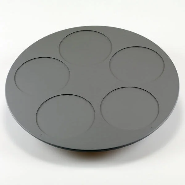
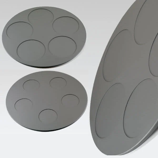
For thin film deposition phases such as epitaxy or MOCVD, Mersen supplies ultra-pure graphite equipment used to support substrates or "wafers". At the core of the process, this equipment, epitaxy susceptors or satellite platforms for the MOCVD, are first subjected to the deposition environment:
- High temperature.
- High vacuum.
- Use of aggressive gaseous precursors.
- Zero contamination, absence of peeling.
- Resistance to strong acids during cleaning operations
-
Ion implant
The ion implantation technique is used in the semi-conductor industry to locally modify the composition and physical properties of a substrate, especially when doping agents such as boron, phosphorus and arsenic introduced…
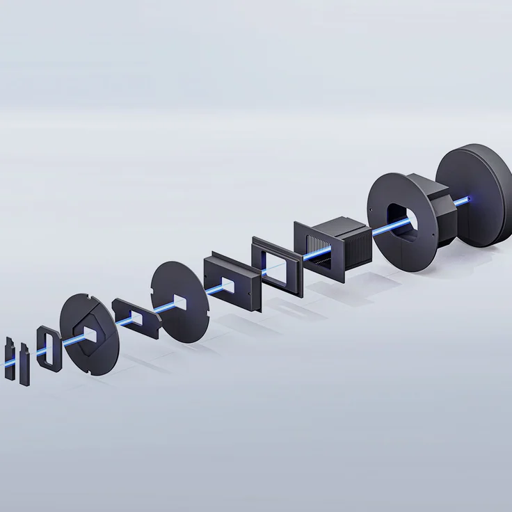
The electrodes and graphite protective screens on these machines are subjected to significant erosion caused by ion bombardment.
Mersen's fine grain and high-density ultra-pure graphite resists erosion very well.
Mersen has also developed a Vitreous Carbon Impregnation "VCI", to further enhance the strength of these parts, while reducing particle emissions.

-
Ultra-pure graphite coated with silicon carbide
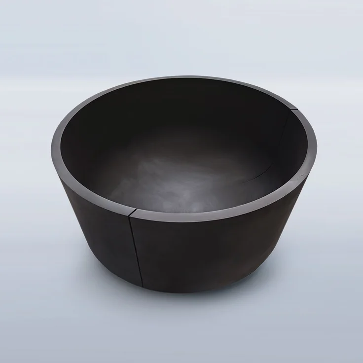
Mersen proposes equipment made of ultra-pure graphite coated with silicon carbide.
These dedicated solutions are the fruit of our expertise in materials and precision machining:- Ultra-pure graphite grades checked by ETV-ICP.
- The compatibility (CTE) of our graphite grades with silicon carbide guarantees long term integrity of the protective coating.
- Our precision machining process undergoes three-dimensional examination to ensure that the design of highly complex parts is respected.
-
Mersen in the semiconductor manufacturing process
-
Product Literature
Technical documentation
ETV-ICP OES - detecting limits for high purity carbon and graphite
pdf - 1.82 MB | Nov. 28, 2024
Purified graphite silicon carbide graphite enhancement
pdf - 2.09 MB | Nov. 28, 2024
Brochures and Flyers
Advanced materials for the photovoltaic (PV) industry
pdf - 11.12 MB | Oct. 16, 2025


